 | –≠–ª–µ–∫—Ç—Ä–æ–Ω–Ω—ã–π –∫–æ–º–ø–æ–Ω–µ–Ω—Ç: S3P863A | –°–∫–∞—á–∞—Ç—å:  PDF PDF  ZIP ZIP |
Document Outline
- s3c8639_rev.2.1_072001.pdf

S3C8639/C863A/P863A/C8647/F8647
PRODUCT OVERVIEW
1-1
1
PRODUCT OVERVIEW
SAM8 PRODUCT FAMILY
Samsung's SAM8 family of 8-bit single-chip CMOS microcontrollers offers a fast and efficient CPU with a wide
range of integrated peripherals, in various mask-programmable ROM sizes. Analog its major CPU features are:
-- Efficient register-oriented architecture
-- Selectable CPU clock sources
-- Idle and Stop power-down mode release by interrupt
-- Built-in basic timer with watchdog function
The sophisticated interrupt structure recognizes up to eight interrupt levels. Each level can have one or more
interrupt sources and vectors. Fast interrupt processing (within a minimum of four CPU clocks) can be assigned
to specific interrupt levels.
S3C8639/C863A/P863A MICROCONTROLLERS
S3C8639/C863A/P863A single-chip 8-bit
microcontrollers are based on the powerful SAM8
CPU architecture. The internal register file is logically
expanded to increase the on-chip register space.
S3C8639/C863A/P863A contain 32/48 Kbytes of on-
chip program ROM.
In line with Samsung's modular design approach, the
following peripherals are integrated with the SAM8
core:
-- Four programmable I/O ports (total 27 pins)
-- One 8-bit basic timer for oscillation stabilization
and watchdog functions
-- One 8-bit general-purpose timer/counter with
selectable clock sources
-- One interval timer
-- One 12-bit counter with selectable clock sources,
including Hsync or Csync input
-- PWM block with seven 8-bit PWM circuits
-- Sync processor block (for Vsync and Hsync I/O,
Csync input, and Clamp signal output)
-- DDC Multi-master and slave-only IIC-Bus
-- 4-channel A/D converter (8-bit resolution)
S3C8639/C863A/P863A are a versatile
microcontrollers which are ideal for use in multi-sync
monitors or in general-purpose applications that
require sophisticated timer/counter, PWM, sync
signal processing, A/D converter, and multi-master
IIC-bus support with DDC. They are available in a
42-pin SDIP or a 44-pin QFP package.
OTP
S3C8639/C863A microcontrollers are also available in OTP (One Time Programmable) version named,
S3P863A. S3P863A microcontroller has an on-chip 48-Kbyte one-time-programmable EPROM instead of
masked ROM. S3P863A is comparable to S3C8639/C863A, both in function and pin configuration except its
ROM size.

PRODUCT OVERVIEW
S3C8639/C863A/P863A/C8647/F8647
1-2
S3C8647/F8647 MICROCONTROLLERS
S3C8647/F8647 single-chip 8-bit microcontrollers are
based on the powerful SAM8 CPU architecture. The
internal register file is logically expanded to increase
the on-chip register space.
S3C8647/F8647 contain 24 Kbytes of on-chip
program ROM.
In line with Samsung's modular design approach, the
following peripherals are integrated with the SAM8
core:
-- Three programmable I/O ports (total 19 pins)
-- One 8-bit basic timer for oscillation stabilization
and watchdog functions
-- One 8-bit general-purpose timer/counter with
selectable clock sources
-- One interval timer
-- One 12-bit counter with selectable clock sources,
including Hsync or Csync input
-- PWM block with six 8-bit PWM circuits
-- Sync processor block (for Vsync and Hsync I/O,
Csync input, and Clamp signal output)
-- DDC Multi-master IIC-Bus
-- 4-channel A/D converter (4-bit resolution)
S3C8647/F8647 are a versatile microcontrollers
which are ideal for use in multi-sync monitors or in
general-purpose applications that require
sophisticated timer/counter, PWM, sync signal
processing, A/D converter, and multi-master IIC-bus
support with DDC. They are available in a 32-pin
SDIP/SOP package.
FLASH
S3C8647 microcontroller is also available in Flash version named, S3F8647. S3F8647 microcontroller has an
on-chip 24-Kbyte flash cells instead of masked ROM. S3F8647 is comparable to S3C8647, both in function and
pin configuration.

S3C8639/C863A/P863A/C8647/F8647
PRODUCT OVERVIEW
1-3
FEATURES
CPU
∑
SAM88RC CPU core
Memory
∑
S3C8639: 32-Kbyte program memory (ROM)
S3C863A: 48-Kbyte program memory (ROM)
S3C8647: 24-Kbyte program memory (ROM)
∑
S3C8639: 784-byte general-purpose
register area
S3C863A: 1040-byte general-purpose
register area
S3C8647: 400-byte general-purpose
register area
Instruction Set
∑
78 instructions
∑
IDLE and STOP instructions added for
power-down modes
Instruction Execution Time
∑
Minimum 333 ns (with 12 MHz CPU clock)
Interrupts
∑
Ten (nine)* interrupt sources/vectors (S3C8647)*
∑
Eight (seven)* interrupt level (S3C8647)*
∑
Fast interrupt feature
General I/O
∑
S3C863X: four I/O ports (total 27pins)
S3C8647: three I/O ports (total 19pins)
8-Bit Basic Timer
∑
Programmable timer for oscillation stabilization
interval control or watchdog timer function
∑
Three selective internal clock frequencies
Timer/Counters
∑
One 8-bit Timer/Counter with several clock
sources (Capture mode)
∑
One 12-bit Counter with H-/C-sync and several
clock sources
∑
One Interval Timer
Low Voltage Detector (LVD & POR)
Pulse Width Modulator (PWM)
∑
8-bit PWM: 7(6)*-Ch (S3C8647)*
(6-bit basic frame with 2-bit extension)
Sync-Processor Block
∑
Vsync-I, Hsync-I, Csync-I input and Vsync-O,
Hsync-O, Clamp-O output pins
∑
Programmable Pseudo sync signal generation
∑
Auto SOG detection
∑
Auto H-/V-sync polarity detection
∑
Composite sync detection
DDC Multi-Master IIC-Bus 1-Ch
∑
Serial Peripheral Interface
∑
Support for Display Data Channel
(DDC1/DDC2B/DDC2Bi/DDC2B+)
Slave Only IIC-Bus 1-Ch (Only S3C863X)
∑
Serial Peripheral Interface
A/D Converter
∑
4-channel; 8(4)*-bit resolution (S3C8647)*
Oscillator Frequency
∑
8 MHz to 12 MHz crystal operation
∑
Internal Max. 12 MHz CPU clock
Operating Temperature Range
∑
≠ 40
∞
C to + 85
∞
C
Operating Voltage Range
∑
3.0(4.0)* V to 5.5 V (S3C8647)*
Package Types
∑
S3C863X: 42-pin SDIP, 44-pin QFP
S3C8647: 32-pin SDIP, 32-pin SOP
PRODUCT OVERVIEW
S3C8639/C863A/P863A/C8647/F8647
1-4
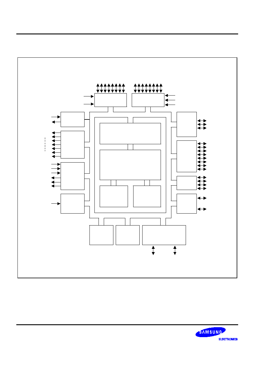
BLOCK DIAGRAM
Port 0
P0.0-P0.7/INT0-INT2
I/O Port and Interrupt
Control
32/48-
Kbyte
ROM
784/1040-
Byte
Register File
SAM8 CPU
Port 2
Port 1
P1.0-P1.2
P2.0-P2.7
V
DD1
, V
DD2
V
SS1
, V
SS2
TEST
RESET
INT0-INT2
ADC
Port 3
P3.0-P3.7
Slave
Only
IIC-Bus
AD0-AD3
SCL1
SDA1
Main
Osc
8-Bit
PWM
(7-Ch)
Sync-
Processor
X
OUT
X
IN
PWM0
PWM6
8-Bit
Counter
(Timer M0)
TM0CAP
Vsync-I
Hsync-I
Csync-I
Vsync-O
Hsync-O
Clamp-O
12-Bit
Counter
(Timer M1)
Interval
Timer
(Timer M2)
Multi-master IIC-Bus
and DDC1/2B/2Bi/2B+
SCL0
SDA0
* S3C8639
- 32 Kbyte ROM
- 784 Byte RAM
* S3C863A
- 48 Kbyte ROM
- 1040 Byte RAM
Figure 1-1. Block Diagram (S3C863X)
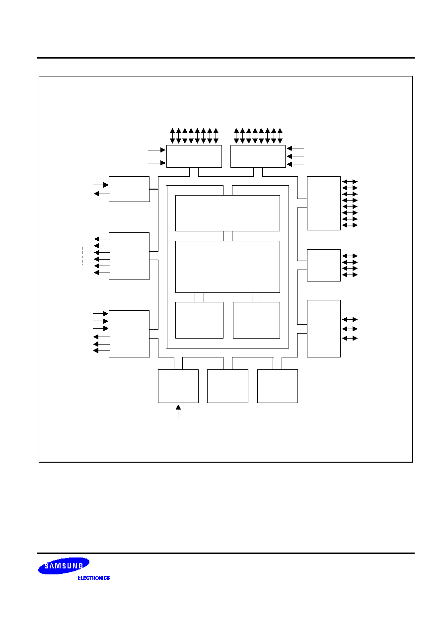
S3C8639/C863A/P863A/C8647/F8647
PRODUCT OVERVIEW
1-5
Port 0
P0.0-P0.2, P0.4/
INT0-INT2
I/O Port and Interrupt
Control
32/48-Kbyte
ROM
400-Byte
Register File
SAM8 CPU
Port 2
P2.0-P2.5,
P2.7
V
DD
V
SS
TEST
RESET
INT0-INT2
8-Bit
Counter
(Timer M0)
Interval
Timer
(Timer M2)
MT0CAP
Sync-
Processor
Vsync-I
Hsync-I
Csync-I
Vsync-O
Hsync-O
Clamp-O
8-Bit
PWM
(6-Ch)
PWM0
PWM5
Main
Osc
X
OUT
X
IN
Port 3
P3.0-P3.7
Multi-
master
IIC-bus
(DDC1/
2B/2Bi/
2B+)
SCL0
VCLK
SDA0
12-Bit
Counter
(Timer M1)
ADC
AD0-AD3
Figure 1-2. Block Diagram (S3C8647)